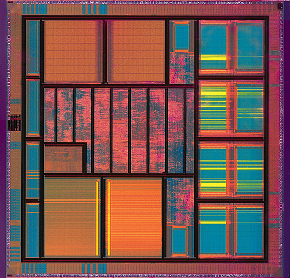


- JDA1 Integrated PLL Eliminates Audio Clock Generation Logic in Multimedia Applications
- JDA1 Eliminates need for Mixed-Signal based Switched-Capacitor Filter Technology
The incorporation of an integrated Phase Lock Loop (PLL) with D/A conversion (DAC) enables the JDA1 to support multiple audio sample rates from a single 27MHz input clock frequency. This eliminates the expense of audio clock generation circuitry normally required for MPEG and other multi-sample-rate applications. In applications incorporating MPEG video, the 27 MHz clock frequency can be shared with the ?STC? and video encoder clocks, further reducing cost. The JDA1 employs all digital PLL circuitry in a novel architecture such that the output oversampling rate is constant over all of the audio sample rates. This results in a constant delta-sigma noise spectrum that can be efficiently filtered regardless of sample rate. Thus the JDA1 provides better performance than traditional designs that simply use a PLL to generate a DAC master clock that is a multiple of the audio sample rate, and thus have noise spectrums that change with sample rate.
By utilizing an all digital design approach, the JDA1 eliminates the requirement for mixed-signal based switched-capacitor filter technology. Switched capacitor output filters have traditionally been utilized by CD quality audio DAC manufacturers, but they typically require special process technology (two layers of polysilicon), and custom layouts, which are not compatible with lower cost ASIC technology used for most VLSI designs. In the past, these mixed-signal constraints have prevented the use of audio DAC functions in low cost VLSI designs. With the introduction of the JDA1 technology, audio DAC and PLL functions can be integrated in VLSI designs, thus reducing cost by eliminating external DAC and and PLL board components. Because the JDA1 uses standard ASIC processes and off-the-shelf libraries, it is easily ported to advanced processes with a minimum of effort for future generation products.
The JDA1 features soft muting and 95dB volume control in 1dB steps. Optional serial interfaces provide SPDIF output and I2C or I2S compatible control and PCM input.
The performance of the JDA1 audio DAC design has been proven in stand-alone and large audio/video integrated applications. The measured dynamic range is in excess of 98 dB (flat, 20 - 20kHz) with THD measured at better than 90 dB below fullscale. SNR is >100dB.
The JDA1 requires very little silicon area. It consists of a single logic block and a 1-Port SRAM, and can be built from off-the-shelf gate array or standard cell libraries. Typical size in 0.35u CMOS technology is only 1.25mm2. The JDA1 design kit is compatible with Synopsys and Verilog design methodologies.
About JPI: JPI is a VLSI design firm specializing in high volume, cost sensitive, consumer audio IC designs. Its designs for DAC, PLL, AC-3, and MPEG applications have been licensed and employed by semiconductor and system manufacturers of audio solutions for the consumer and computing markets. Founded in 1995, JPI is a California Corporation with operating facilities in Oakland and San Francisco. More information can be obtained on their web site at http://www.jacobspineda.com.
For Information Contact: Steven A. Brightfield Centamicron, Inc. (415) 948-9293 brighty@jacobspineda.com
(c) 1997 Jacobs Pineda, Inc. All rights reserved.