

FEATURES
PRODUCT DESCRIPTION
The JDA1 is a digital-to-analog converter core cell suitable for all high quality
audio and multimedia applications. The JDA1 accepts 24-bit PCM input at one
of four selectable standard audio sample rates to produces stereo analog outputs.
The JDA1 internally generates the audio sample clocks from a single 27MHz clock
input, which would typically be derived from the 27MHz video/STC frequency available
in MPEG based systems. The JDA1 is a fully digital Sigma-Delta converter that
produces a pulsed output, which can work with off-chip filtering to produce
analog output. The JDA1 can also work with on-chip switched-capacitor filter
circuitry, however the pulsed output configuration is more economical for highly
integrated VLSI applications. The JDA1 is targeted to a variety of applications
such as
digital set-top boxes, MPEG/Dolby Digital/MP3 capable equipment.
The JDA1 contains three main processing blocks. The first is an interpolation filter engine, which increases the sample rate of the input PCM signal to 8fs, providing approximately 65dB of image rejection. The second block performs noise-shaping and pulse shaping. The third block is a Phase-Lock Loop (PLL) to derive timing from the master clock.
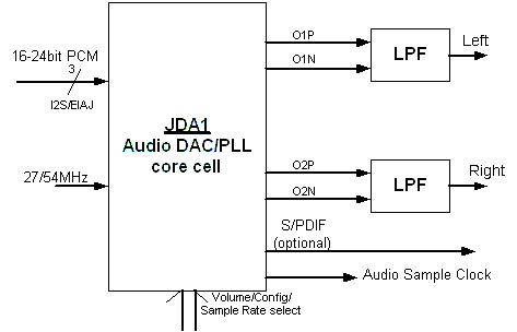
Several interfaces (I/F) are available for the JDA1. A 3-wire serial PCM input interface allows standard 3-wire serial digital audio signals (up to 24-bit wordlengths) to be fed to the JDA1. On a larger IC, such as an audio decompression IC, the input to the JDA would most likely be in parallel words, eliminating the need for a serial interface. An S/PDIF formatter allows formatting the input stereo PCM samples into the single-wire format used to send digital audio signals between audio products. This is programmable, allowing the transmission of compressed data also, as specified by Dolby Laboratories for Dolby Digital/AC-3 signals. Finally, simple 3-wire or I2C microprocessor interfaces are available for setting of volume, muting, and other configuration bits inside the JDA1 from a host processor.
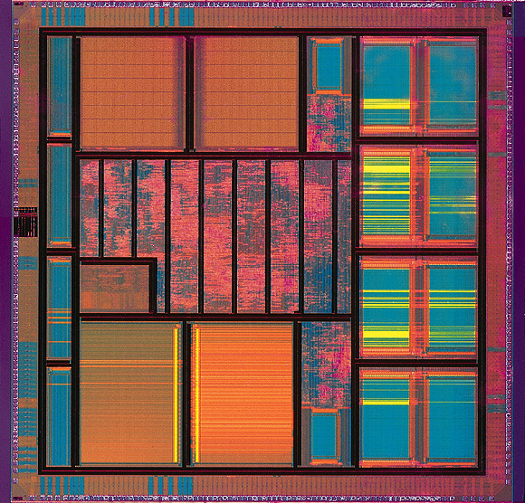
The JDA1 is very efficient in silicon area, requiring only 0.7- 1.0 mm2 in a standard CMOS process with design rules of 0.25u. Estimated size in 0.18u libraries is 0.50 - 0.6mm2. This includes all logic, RAM and ROM necessary for the signal processing. No custom cell libraries are required. The JDA1 follows the Verilog/Synopsys design flow for easy porting to new libraries.
APPLICATIONS
The JDA1 DAC is suitable for digital audio VLSI applications that operate at audio sampling rates of 32 kHz, 44.056 kHz, 44.1 kHz and 48kHz and require analog outputs. The JDA1 produces stereo outputs from a standard 2-channel digital input. Its built in PCM interface is a 20-bit parallel bus that interfaces directly to a digital audio source. A serial 3-wire interface (up to 24-bit PCM samples) may be used as well, to interface to devices supplying PCM in a variety of serial formats such as Philips I2S or EIAJ 16 to 24 bit right justified. An optional digital output module supplies data in S/PDIF format. The JDA1 now supports MPEG half-rate audio sample rates (as a configurable option), which are sub-multiples of 2 of the standard three audio rates: 16kHz, 22.05kHz, and 24kHz. Operation at 96kHz is also possible using a 54MHz master clock rates.
Control of the JDA1 operating modes and features, such as volume control and muting, are handled by a control bus input. This may be driven by optional host interfaces. In a typical VLSI application, there is usually a single host interface that supplies all of the modules on the IC, and the JDA1 can simply act as a client of this interface.
The oversampled output is differential and can be interfaced to switched capacitor on-chip filter or an external buffer to generate a single ended audio output. Analog filter rolloff at 20 kHz is compensated by the internal digital filters.
JDA1 uses a single low-jitter 27 MHz clock input from which all audio frequencies needed by the DAC are internally derived. The incorporation of an integrated Phase Lock Loop (PLL) with D/A conversion(DAC) enables the JDA1 to support multiple audio sample rates from the single input clock frequency. This eliminates the expense of audio clock generation circuitry typically required in MPEG and other multi-sample-rate applications.
AUDIO CLOCK GENERATION
The JDA1 internally derives the audio sample clock directly from the 27MHz master clock, and supplies this as an output to clock digital data from the audio source. The JDA1 also outputs 128 x fs and 256 x fs frequencies for use by other circuits such as an S/PDIF formatter (See IEC 60958 standard). With the half-rate option configured, the JDA1 may be programmed to output either 128x and 256x clocks to support half-rate SPDIF (as emerging in AES3 and IEC60958 standards), or 256x and 512x clocks to support sending compressed MPEG data via SPDIF as specified in IEC61937 (which may be needed in applications with an audio decoder such as the J1).
AUDIO PERFORMANCE
Audio performance measurements were taken on a stand-alone application of the JDA1. The test conditions are listed in Table 2. All filters used are internal to the Audio Precision analyzer, with the exception of an external 20 kHz brickwall lowpass filter used for measuring Dynamic Range and THD+N vs. Amplitude. A summary of the audio performance is given in Table 3.
TEST RESULTS SUMMARY
The frequency response is extremely flat throughout the audio band; rolloff at 20 kHz is virtually nonexistent. Passband ripple, amplitude imbalance, and phase imbalance are all negligible.
The THD+N at 1 kHz is better than 90 dB (.003%) when measured with the external 20 kHz brickwall lowpass filter. The THD+N at -60 dBFS is -33.8 dB with 16 bit data, improving to -37.9 dB with 18 bit data. The calculated dynamic ranges are 93.8 dB and 97.9 dB, respectively.
Signal to noise ratio at digital silence exceeds 100 dB. Crosstalk is nearly -120 dB at 1 kHz but drops to -92 dB at 20 kHz, possibly because of eval board layout. The JDA1 has been shown to maintain very good signal-to-noise ratios of > 100dB even in large VLSI applications, where it resides on the same silicon die as audio, video decoders, etc. totalling near 250,000 gates.
TECHNOLOGY COMPATIBILITY
An advantage of the JDA1 architecture is that it consists of entirely digital signal processing circuitry and as such, it is compatible with other digital circuitry and VLSI processes. Sigma-delta converters such as the JDA1 are by nature mostly digital. Figure 1 shows a typical sigma-delta stand-alone DAC, which consists of the digital processing circuitry to raise the sample rate and perform noise shaping. After noise shaping, most manufacturers exploit sampled-data switched-capacitor filtering to attenuate the high frequency noise of the oversampled signal and provide an analog signal output. This configuration has the advantage that all of the analog circuitry is integrated onto the IC. However, it also has a disadvantage that the analog circuitry needs an analog process technology that supports two poly layers which are necessary for manufacturing efficient capacitors. Unfortunately, analog processes typically lag processes for all-digital VLSI design rules, and they are offered by only a limited number of ASIC vendors. Further, analog circuitry requires non-portable custom layouts specific to the process design rules. Consequently this level of integration is generally not compatible with VLSI applications where the DAC is combined with other digital functions.

The JDA1 architecture is suitable for integration with switched capacitor output filtering as well. However, in addition, the JDA1 design supports a more economical pulse density modulated output mode which does not use on-chip switched capacitor circuitry at all. In this mode of operation, the analog signal is recovered from the pulse density output by a two pole filter incorporated into the external buffer amplifier typically present in a board level design to drive output signal levels. This partitioning has a great advantage for large VLSI applications because it enables the intergration of the DAC onto a large VLSI chip without the need for special analog processes, and further eliminates the cost of the on-chip analog circuitry. The added cost of the external two pole filter is nominal because it is implemented simply by the addition of a small number of passive components to the feedback path of the external buffer amplifier.
Another design consideration is the sensitivity to clock jitter, which has the effect of modulating the output amplitude by affecting the width of the output pulses. The JDA1 clock input should come from a low jitter clock source. For this reason, the JDA1 is designed to operate from the 13.5 or 27 MHz STC/video frequency which is commonly generated by a VCXO in MPEG based systems. Because JDA1 uses this already available clock frequency, it actually eliminates the audio crystal typically needed in MPEG systems, further reducing system cost. Other master clock frequencies may be supported upon customer request.
Audio Sample Rate Capabilities:
The JDA1 is currently designed to support 8 audio sample rates. These sample rates are shown in Table 1 along with the appropriate divisors to use in generating the respective 256fs rate clocks from the 27 MHz source. When a 54MHz master clock is used, then rates are doubled, allowing 96Khz operation.
| Mode | Sample Rate (fs) | Timebase (T) | Divisor (M) | T/M = 256fs |
| DVD | 48 KHz | 27 MHz | 1125/512 | 12.2880 MHz |
| CD | 44.1 KHz | 27 MHz | 1875/784 | 11.2896 MHz |
| TV | 44.056 KHz | 27 MHz | 2145/896 | 11.2783 MHz |
| Lo-Fi | 32 KHz | 27 MHz | 3375/1024 | 8.1920 MHz |
| Syncrhonous | 52.734kHz | 27MHz | 2.000000 | 13.5 MHz |
| CD half-rate* | 22.05kHz | 27MHz | 3750/784 | 5.6448 MHz |
| DVD half-rate* | 24.0kHz | 27MHz | 2250/512 | 6.144 MHz |
| Lo-Fi half-rate* | 16kHz | 27MHz | 6750/1024 | 4.096 MHz |
*When configured with the JDA1 half-rate option. The JDA1 may be customized to other sample rates upon request.
TEST CONDITIONS FOR JDA1 MEASURED PERFORMANCE
|
|
||||||||||||||
| Parameter |
|
|
Filter | |||||||||||
| Output Level |
|
|
||||||||||||
| Amplitude vs. Frequency |
|
|
||||||||||||
| L/R Amplitude Imbalance |
|
|
||||||||||||
| L/R Phase Imbalance |
|
|
||||||||||||
| Total Harmonic Distortion + Noise | ||||||||||||||
| (THD+N) | at 1kHz |
|
|
22 kHz LPF | ||||||||||
| vs. Freq. |
|
|
20 kHz LPF | |||||||||||
| Total Harmonic Distortion + Noise | ||||||||||||||
| (THD+N) | vs. Ampli. |
|
|
22 kHz LPF | ||||||||||
| 20 kHz LPF (external) | ||||||||||||||
| Dynamic Range |
|
|
22 kHz LPF | |||||||||||
| 20 kHz LPF (external) | ||||||||||||||
| IMD (CCIF 400 Hz & 4080 Hz) |
|
|
80 Hz BPF | |||||||||||
| L/R Crosstalk (Isolation) |
|
|
BPF at Fundamental | |||||||||||
| Signal to Noise Ratio (SNR) |
|
|
22 kHz LPF | |||||||||||
| (Digital Silence) | ||||||||||||||
| Digital Audio Generator | FFT Analyzer Settings | |||||||||||||
| Data Length: | 16 bits | Record Length: | 16384 | |||||||||||
| Data Format: | SPDIF | Averages: | 16 | |||||||||||
| Sampling Rate (Fs): | 44.1 kHz | Filters: | 20 kHz LPF (external) | |||||||||||
| Bit Clock | 64*Fs | Windows: | Hann | |||||||||||
| System Clock: | 27.0 MHz | Sampling Rate: | 44.1 kHz | |||||||||||
| Dithering: | ON (Rectangular) | Trigger: | Auto | |||||||||||
MEASURED AUDIO PERFORMANCE FIGURES
| Table 3 - Typical Measured Audio Performance | Vdd=5V | ||||||||||
|
|
|||||||||||
| Parameter |
|
|
|
||||||||
| Output Level |
|
|
|
||||||||
| Amplitude vs. Frequency |
|
|
|
||||||||
| L/R Amplitude Imbalance |
|
|
|
||||||||
| L/R Phase Imbalance |
|
|
|
||||||||
| (THD+N) | at 1 kHz |
|
|
|
|||||||
| vs. Freq. |
|
|
|
||||||||
| Dynamic Range | 16 bit data |
|
|
|
|||||||
| 18 bit data |
|
|
|
||||||||
| IMD (CCIF 4000 Hz & 4080 Hz |
|
|
|
||||||||
| Crosstalk (Isolation): | 1 kHz |
|
|
|
|||||||
| 20 kHz |
|
|
|
||||||||
| Signal to Noise Ration (SNR) |
|
|
|
||||||||
| (Digital Silence) | |||||||||||
DESIGN KIT
The JDA1 design kit is compatible with Synopsys and Verilog design methodology. JDA1 requires 035 micron or better technology, and is designed for synthesis with off-the-shelf gate array or standard cell ASIC libraries. Click here to find out more out the core cell design kit.